


The integrity of a Printed Circuit Board (PCB) is paramount to the functionality of any electronic device. 💡
A broken or damaged trace—the copper pathways that conduct electricity—can lead to intermittent failures or complete system shutdown. 💔
Repairing these microscopic faults requires precision, the right tools, and a methodical approach, transforming a dead board back into a functional component. 🛠️
As the saying goes, “The chain is only as strong as its weakest link,” and on a PCB, a broken trace is exactly that. 🔗
This article outlines the essential techniques and best practices for successfully restoring continuity to a damaged PCB trace, primarily focusing on the robust wire jumper method.
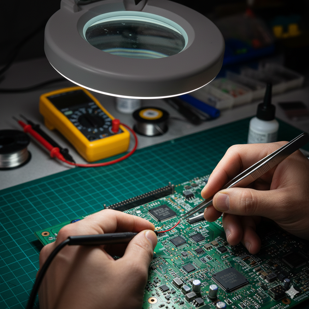
I. Preparation and Inspection: The Foundation of Repair 🔬
Before any repair begins, a thorough inspection and preparation of the damaged area are critical. 📌
Rushing this stage often leads to rushed, unreliable repairs.
A. Locating the Break and Assessing Damage
The first step is to precisely locate the break. 🧐
This is typically done using a multimeter set to continuity mode (the one that beeps).
By probing the trace on either side of the suspected damage, a lack of continuity (an open circuit, indicated by ‘OL’ or no beep) confirms the break. 💔
For breaks that are not visibly obvious, you may need to check continuity between two known points on the same trace, gradually moving closer until the continuity disappears.
Once the break is located, assess the extent of the damage.
Is it a clean break, or has a large section of the trace been lifted or burned? 🔥
This assessment determines the required length of your jumper wire.
B. Cleaning and Exposing the Bare Copper Trace
The area around the break must be meticulously cleaned and the protective coating removed. ✨
The solder mask, a protective polymer coating, must be gently removed to expose the bare copper trace on both sides of the break, creating a clean anchor point for soldering.
| Tool | Purpose | Technique |
|---|---|---|
| Fiberglass Brush | Removing oxidation and light contaminants. | Gentle scrubbing motion, light pressure. |
| Hobby Knife/Scalpel | Carefully scraping away the solder mask. | Scrape lightly to avoid damaging the copper trace underneath. |
| Rotary Tool (Dremel) | Controlled, gentle removal of the solder mask over a larger area. | Use a fine grinding bit, held lightly and at low speed [2]. |
| Isopropyl Alcohol (IPA) | Final cleaning of the exposed copper and surrounding area. | Use a cotton swab or lint-free cloth to remove debris. |
The copper exposed should be shiny and clean to ensure the solder adheres correctly.
II. Repair Techniques: Bridging the Gap 🌉
The choice of repair technique depends on the width of the trace, the current it carries, and the severity of the damage.
For most traces, the wire jumper method is the most common, robust, and reliable solution.
A. The Wire Jumper Method: The Gold Standard
This technique involves soldering a fine, insulated wire across the break to restore the electrical connection, effectively creating a new pathway. 🚧
- 1. Tinning the Exposed Trace: Apply a small amount of flux to the exposed bare copper on both sides of the break. Then, apply a thin layer of solder (tinning) to prepare the surface for the jumper wire. This step is crucial for achieving a strong solder joint.
- 2. Preparing the Jumper Wire: Use a fine-gauge, insulated wire, such as 30 AWG wire-wrap wire. The insulation prevents accidental shorts to adjacent components or traces. Strip a very small amount of insulation (about 1 mm) from both ends. For long runs, the insulation must remain to prevent short circuits.
- 3. Soldering the Jumper: Solder one end of the prepared wire to the tinned copper on one side of the break. Ensure a solid, low-profile solder joint that minimizes bulk. The insulation should butt right up to the solder joint.
- 4. Routing and Securing: Route the wire neatly across the damaged area to the other side. Solder the second end to the tinned copper, ensuring the wire is taut but not stressed. Use Kapton tape or a small dab of adhesive for long runs to prevent the wire from lifting and causing future issues.
- 5. Continuity Check: The final test before protection! Use the multimeter to confirm robust continuity across the newly installed jumper. You should get a solid beep or a reading very close to zero Ohms (\Omega).
https://youtu.be/p60Q6z-0Q1s
B. Alternatives: Conductive Ink or Copper Foil
While the wire jumper is preferred for reliability, two other methods are sometimes used.
For very fine, low-current traces, specialized conductive pens or epoxies can be used.
These methods are generally less robust than a wire jumper and are often reserved for temporary fixes or specialized repairs where a wire simply won’t fit.
Another option is using a piece of thin copper foil (like those from a PCB repair kit) that is glued and then soldered over the break.
This provides a wider conductor but can be tricky to secure and insulate properly on a dense board.
“If you do it right the first time, you won’t have to do it again,” is a principle that applies here, making the wire jumper the preferred reliable route.
Choose the wire gauge carefully; a trace carrying significant power will require a thicker wire to avoid creating a fuse! ⚡
III. Post-Repair Protection: Securing the Fix 🛡️
Once the electrical continuity is confirmed, the repair must be protected from environmental factors and mechanical stress to ensure long-term reliability.
The repair is not complete until this step is done.
- 1. Cleaning: Remove any residual flux using IPA (Isopropyl Alcohol) and a small, stiff brush. Flux residue can be corrosive over time and is tacky, attracting dust and grime. 🦠
- 2. Applying Solder Mask: Apply a UV-curable solder mask or a specialized PCB lacquer over the entire repair area, including the wire and the solder joints. This step is vital as it restores the protective layer. The solder mask prevents oxidation of the copper and secures the jumper wire in place.
- 3. Curing: Cure the solder mask using a UV lamp or natural sunlight, following the product instructions. Most UV masks cure quickly under a dedicated UV light source. This process hardens the mask into a durable, protective shell.
https://youtu.be/P5zU0-L29y4
IV. Essential Tools and Best Practices ⚙️
The right tools and disciplined practices are non-negotiable for successful PCB trace repair.
A. Critical Equipment Checklist
- Magnification: A microscope or a high-quality magnifying lamp is essential, as the work is often microscopic.
- Soldering Iron: A temperature-controlled soldering station with a fine-point tip (a chisel tip for tinning, a conical tip for fine wire).
- Multimeter: For continuity checks (before and after the repair).
- Chemicals: No-clean flux, Isopropyl Alcohol (IPA), and UV-curable solder mask.
- Wire: Fine-gauge insulated wire (30 AWG Kynar wire-wrap wire is standard).
B. Best Practices for Micro-Repair
Remember that heat management is paramount. 🔥
Use the lowest soldering iron temperature that reliably melts the solder to prevent lifting nearby traces or damaging sensitive components.
Always anchor the board securely in a sturdy holder (e.g., a “third hand”) to prevent movement.
Before you even begin, practice makes perfect. 🤓
Try the wire jumper technique on a scrap board first.
As Confucius wisely stated, “By three methods we may learn wisdom: First, by reflection, which is noblest; Second, by imitation, which is easiest; and third by experience, which is the bitterest.” Experience here means practice before the live repair!
https://youtu.be/M-YlXkP_2S0
V. When to Avoid DIY Repair 🛑
Not every broken trace should be a DIY project.
If the damage is on a multi-layer board (where internal layers are damaged), or if the break is directly under a Ball Grid Array (BGA) component, the repair requires professional rework stations and specialized expertise.
Attempting these complex repairs without the proper equipment can lead to irreversible damage to the board.
Know your limits and consult a professional technician when necessary.
Focus on single-layer or external-layer trace breaks for reliable home or bench repairs.
VI. Essential External Resources 📚
For more detailed information and advanced troubleshooting:
Chemtronics: HOW-TO: PCB Trace Repair With a Wire Jumper
Hackaday: Five Ways To Repair Broken PCB Traces
AllPCB: The Ultimate Guide to PCB Trace Repair: Step by Step for Engineers
IPC (Association Connecting Electronics Industries) Repair Standards
Electronic Design: How to Do PCB Repair and Modification
Conclusion ✨
By following these meticulous steps—from precise location and careful cleaning to the final protection with solder mask—technicians and hobbyists alike can reliably repair broken PCB traces, extending the life and functionality of valuable electronic hardware. 🥳
Mastering the wire jumper technique is a cornerstone skill in electronics maintenance and repair.
Take your time, be precise, and restore that vital electrical connection! 🔌
The ability to fix a broken trace can save both time and money, proving the value of a steady hand and methodical process.