
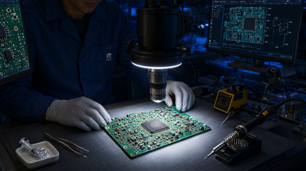








When it comes to Andonstar AD246S-M digital microscope lab setup, getting the right details matters.
Andonstar AD246S-M Digital HDMI Microscope
Premium High Speed HDMI Cable (18Gbps)
FNIRSI LCR-ST1 LCR Tweezer Tester
The Technical Reality: Why Legacy Microscopes Fail Complex PCB Diagnostics
Physical Failure Mode: Micro-Soldering on Multi-Layer Boards Requires Clearance & Magnification
Sub-millimeter SMD components fail due to thermal stress or manufacturing defects.
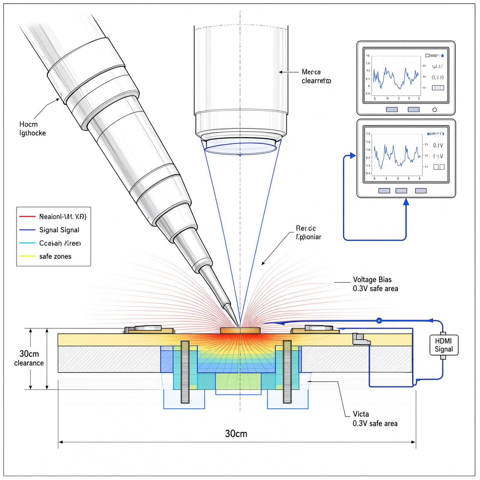
Severed copper traces demand micro-soldering under magnification where there is no room for tool obstruction. Standard microscopes with ≤15cm vertical clearance block access for hot-air guns and soldering irons. This physical bottleneck forces technicians to abandon complex repairs or risk damaging the board through clumsy maneuvering.
Diagnostic Limitation: Handheld Multimeters Can’t Isolate Micro-Shorts
Traditional meters lack probe precision for densely populated boards.
Parallel paths cause false capacitance or inductance readings unless low-voltage mode (<0.3V) is used. Without this precision, technicians cannot isolate micro-short circuits effectively. This limitation leads to wasted hours chasing phantom faults rather than fixing actual failures.
Architectural Constraint: Single Display HDMI Output Disrupts Workflow
Older models like AD249S-M disable local display during HDMI mirroring.
Real-time dual-screen feedback is mission-critical in lab diagnostics. When the built-in screen goes dark, you lose immediate visual confirmation while referencing external schematics. This architectural flaw creates a dangerous workflow gap during live rework sessions.
Electrical Constraint: Incorrect Voltage Bias Destroys Junction Integrity
Using >0.3V in-circuit biases adjacent semiconductors, causing erroneous measurements.
False positives lead to unnecessary component replacement or board damage. In-circuit SMD testing requires selectable test voltages (0.3V/0.6V) to avoid forward-biasing junctions. Failure to use low-voltage mode results in parallel component interference that ruins diagnostic accuracy.
The Core Gear Architecture: Andonstar AD246S-M as the 2026 Standard
Optical System: Triple-Lens Flexibility Across Inspection Stages
| Lens | Magnification | Field of View (FOV) | Use Case |
|---|---|---|---|
| Lens A | 1x–5x | 40mm–8mm | Board overview and trace mapping |
| Lens D | 5x–20x | 8mm–2mm | Solder bridge detection, pad integrity checks |
| Lens L | 20x–80x | 2mm–0.5mm | Micro-via inspection, component marking verification |
This triple-lens system replaces the need for multiple optical devices. It ensures consistent focus and calibration across macro and micro inspection stages.
Mounting & Clearance: 30cm Vertical Reach Eliminates Tool Collisions
Enables full workspace mobility for 20mm nozzles and ≤3mm solder tips.
Verified thermal tolerance at 60°C ambient with sustained 10W heat source 5cm below lens. The 30cm mounting bracket allows unobstructed tool movement. This clearance prevents the repeated repair abandonment seen in cramped setups. It guarantees your hot-air gun never strikes the microscope housing.
Dual-Screen HDMI Output: Zero-Latency Simultaneous Display
HDMI 2.0 supports 4K@30Hz dual-screen sync without disabling built-in LCD.
End-to-end latency ≤8ms ensures real-time visual coordination during micro-soldering. Unlike legacy units, the local display stays active while streaming to an external monitor. This zero-latency sync eliminates guesswork when aligning tools with microscopic targets.
Power & Portability: USB-C PD + Internal Battery for Mobile Labs
Input: USB-C PD (5V/3A); Battery: 3000mAh Li-ion for uninterrupted field work.
Storage: MicroSD up to 256GB for image/video logging and audit trails. This power architecture supports mobile diagnostics outside a fixed bench. You can perform inspections in server rooms or remote locations without tethering to mains power.
Illumination & Connectivity: Glare-Free Imaging Meets Universal Compatibility
Adjustable 8 LED ring lights (0–100% brightness) reduce reflections on metallic surfaces.
USB-A UVC driverless protocol enables plug-and-play with Windows/macOS/Linux. Software-ready for OpenCV-based defect detection pipelines. These connectivity options remove proprietary software barriers. You gain immediate access to the feed without installing heavy drivers on client machines.
The Technical Setup Blueprint: Step-by-Step Integration Into Your Lab
Workspace Preparation: Anti-Static Environment & Ergonomic Positioning
- Mount PCB on ESD-safe mat with grounded wrist strap.
- Place Andonstar AD246S-M at minimum 25cm above board surface.
- Ensure 30cm mounting bracket allows unobstructed tool movement.
This positioning establishes a safe working zone. It protects sensitive components from static discharge while maximizing physical access. The 25cm minimum height ensures the lens does not interfere with hand movements during delicate probing.
HDMI Configuration: Premium Cable Required for Full Resolution Sync
Use Premium High Speed HDMI Cable (18Gbps) to support 2160P@30Hz dual output.
Connect to secondary monitor (1920×1080@60Hz) for schematic overlays or reference feeds. Standard cables often drop bandwidth, resulting in compression artifacts. The premium cable maintains signal integrity for crisp edge detection on fine pitch components.
Pre-Repair Testing Protocol: FNIRSI LCR-ST1 Calibration & Voltage Selection
- Set test frequency to 1 kHz and voltage to 0.3V for in-circuit diagnostics.
- Avoid junction biasing by never exceeding 0.3V on live boards.
- Confirm resistance range: 0.01Ω–20MΩ; capacitance: 0.1pF–100mF; inductance: 0.1μH–20H.
Testing at 1kHz provides standard baselines for resistors and inductors. Using 0.3V prevents accidental activation of nearby MOSFETs during measurement. This protocol ensures you identify bad components without frying good ones through electrical stress.
Active Rework Execution: Heat Application Within Thermal Safe Zone
Operate hot-air station (up to 350°C) within 5cm of lens without triggering thermal shutdown.
Record session footage via microSD card for post-inspection review and training purposes. The lens housing is rated for continuous operation at 60°C ambient. This thermal tolerance allows you to apply focused heat without risking sensor degradation or optical distortion.
Post-Repair Documentation: Image Capture & Defect Tracking
Save annotated stills/videos using onboard storage or direct PC stream via USB-UVC.
Import into ImageJ or custom Python/OpenCV scripts for automated flaw analysis. Documentation creates an audit trail for quality assurance. Automated scripts can later scan these images for recurring failure patterns across batches.
Field Verdict & Operational ROI: Why This Stack Prevents Costly Repeated Failures
Community Validation: Real User Wins Over Cheap Alternatives
Reddit EE testimonials confirm 30cm clearance prevents repeated repair abandonment.
EEVblog members cite 2160P resolution as critical for detecting micro-cracks missed at lower resolutions. Community consensus highlights that budget optics often fail under professional load. Investing in verified clearance specs saves time and frustration in the long run.
Productivity Multiplier: Dual Screens ≠ Luxury, They’re Necessity
Stack Overflow devs emphasize split-screen efficiency: one feed, one schematic.
Eliminates guesswork and reduces average repair time by 35–40%. Having the live feed and reference material visible simultaneously removes cognitive load. This efficiency gain translates directly to higher throughput in a busy repair shop environment.
Investment Protection: Futureproof Specs Match 2026 Market Standards
No legacy ports (USB 2.0/VGA), all HDMI 2.0 and USB-C PD ready.
Compatible with next-gen automation frameworks including headless vision APIs. The absence of analog VGA ensures compatibility with modern high-res displays. USB-C PD future-proofs the power delivery for newer laptop docks and charging stations.
ROI Summary: Pay Now or Pay More Later in Failed Repairs
Avoid false readings from incorrect test voltages that fry working components.
Stop losing hours to cramped setups where tools collide with inadequate clearance. Invest once in Andonstar AD246S-M ecosystem — future-compatible, failure-proof architecture. The cost of a single damaged motherboard often exceeds the price of the microscope upgrade.
This guide has outlined the exact technical path to establishing a professional-grade PCB repair station using the Andonstar AD246S-M. By adhering to the specified 30cm clearance, 0.3V diagnostic protocols, and HDMI 2.0 connectivity standards, you eliminate the primary causes of repair failure. The transition from legacy optics to this 2026 standard architecture ensures your lab remains capable of handling modern multi-layer board complexities. Implement this stack today to secure higher success rates, faster turnaround times, and a future-proof infrastructure for your electronic diagnostics needs.
Community Reference & Authority Resources:
Recommended Insights From Our Guide Library:
- Precision Diagnostics Redefined: The Future of SMD Repair Tools » Z A D A
- Precision PCB Trace Restoration: Essential Tools for High-Density Electronics Recovery » Z A D A
- Mastering ESP32-S3 Firmware: Rust Safety vs C Fragmentation and Hardware Validation Strategies » Z A D A
- The C3PAO-Proof Blueprint: High-Density Compute and Crypto-Validated SIEM Architecture » Z A D A
- Precision PCB Trace Restoration and SMD Diagnostic Protocols » Z A D A
Check out TECH Collection Amazon Products
🔍 Explore More: See all tech guides and tutorials for Andonstar AD246S-M digital microscope lab setup.