
The integrity of a Printed Circuit Board (PCB) is the foundation of any modern electronic device. 🏛️
These boards are the nervous system of electronics, routing signals and power to where they are needed most. ⚡
A broken or damaged trace—the thin copper pathways that conduct electricity across the board—can be disastrous. 💥
It can lead to frustrating intermittent failures, strange device behavior, or a complete system shutdown. 🛑
While it might seem like a death sentence for a device, repairing these microscopic faults is entirely possible. 🛠️
It is a skill that marries art and science, requiring steady hands, precision tools, and a methodical approach. 🔬
Mastering trace repair can save expensive industrial equipment or beloved vintage electronics from the landfill. ♻️
This article outlines the essential techniques, tools, and best practices for successfully restoring continuity to a damaged PCB trace. 📚
I. Understanding Why Traces Fail 🤔
Before diving into the repair, it helps to understand why traces break in the first place. 🧐
Often, the damage is physical. 🔨
A dropped device can cause the PCB to flex, cracking traces near rigid components like heavy inductors or connectors. 📉
Other times, it is accidental damage during a previous repair attempt. 😓
A slip of a screwdriver or overheating a pad during desoldering can easily lift or sever a delicate track. 🔥
Corrosion is another major culprit, especially in devices exposed to moisture or leaking batteries. 💧
The corrosion eats away at the copper until the connection is severed. 🧪
Identifying the root cause can sometimes help prevent future failures after you have completed the repair. 🛡️
II. The Essential Toolkit 🧰
You cannot perform microsurgery with regular mechanics’ tools. 🚫
Successful trace repair requires a specific set of high-quality tools. ✨
Here is what you should have on your bench before starting. 👇
- Precision Soldering Station: A generic, uncontrolled soldering iron will not cut it. You need a temperature-controlled station with a very fine conical or chisel tip (e.g., 0.2mm to 0.5mm). 🌡️
- Quality Flux: Flux is critical for ensuring solder flows onto the oxidized copper quickly without excessive heat. A tacky “no-clean” gel flux is often best for this work. 🍯
- Magnification: These traces are often thinner than a human hair. A good magnifying desk lamp (5x-10x) or, ideally, a stereo microscope is essential for seeing what you are doing. 🔬
- Jumper Wire: You need very fine, insulated copper wire. 30 AWG Kynar-insulated wire-wrap wire is the standard choice for most trace repairs. 🧵
- Scalpel or Hobby Knife: A brand new, extremely sharp #11 blade is necessary for scraping away the solder mask. 🔪
- Fiberglass Scratch Pen: This is excellent for gently abrading the surface to expose copper without cutting too deeply. 🖊️
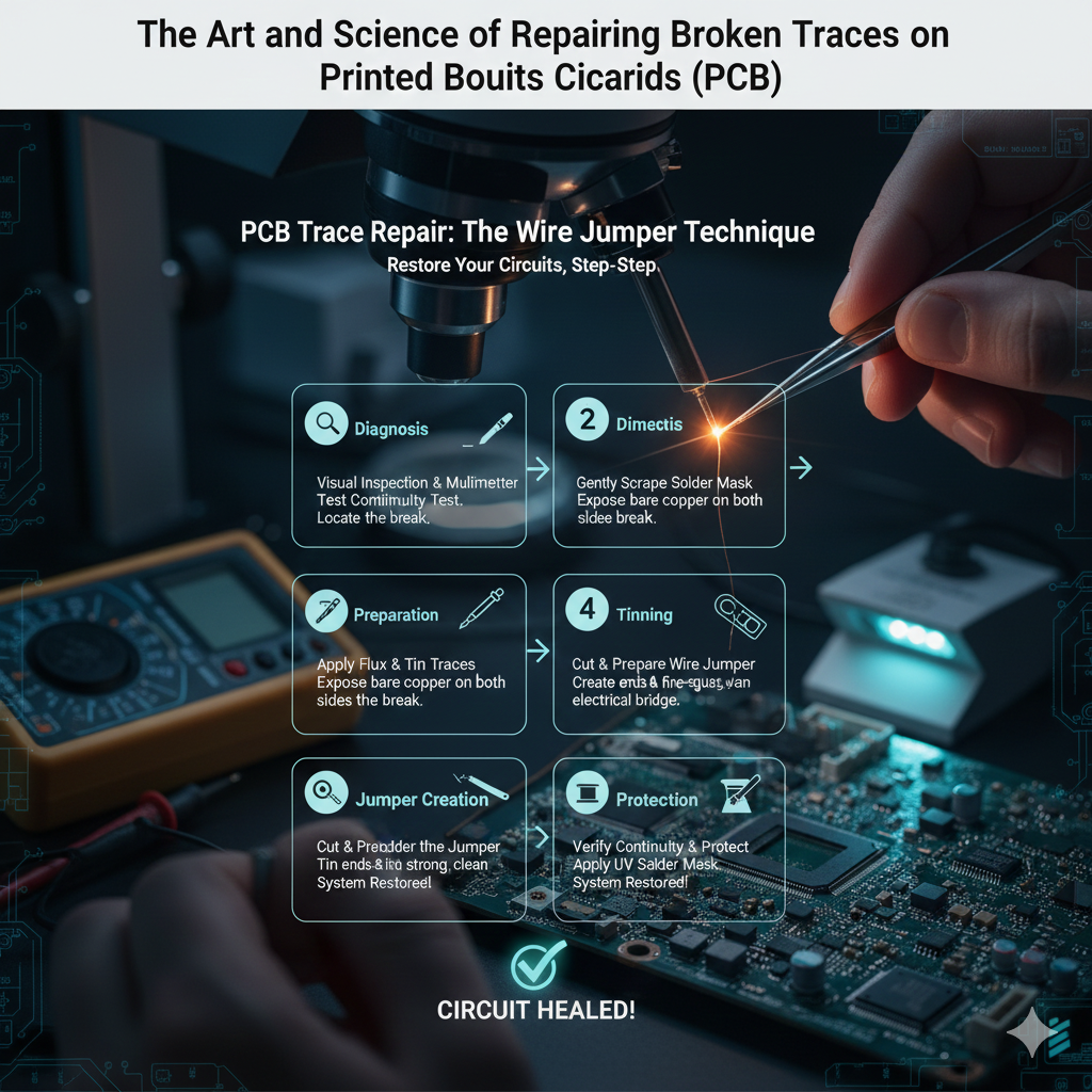
III. Phase 1: Preparation and Inspection 🧐
90% of a good repair is in the preparation. ⏳
Rushing into soldering without properly preparing the area is a recipe for failure. ❌
A. Locating the Break 🔍
Sometimes the break is obvious to the naked eye, like a deep scratch across the board. 👀
Other times, it is a hairline fracture invisible without a microscope. 👻
The first step is to precisely locate the faulty area. 🎯
This is typically done using a high-quality digital multimeter set to continuity mode. 🔊
By probing the trace on known good points on either side of the suspected damage, you can confirm the issue. 📏
A lack of continuity beep (indicating an “open circuit” or OL) confirms the break exists between your probes. 🔇
https://youtu.be/2Ztzt68bA2s
B. Cleaning and Exposing the Trace 🧼
Once located, the area around the break must be meticulously cleaned of dust, grime, or old flux residues. 🧽
Use Isopropyl Alcohol (IPA) of 99% concentration and a lint-free cloth or brush. 💧
Next, you must remove the solder mask. 🎭
The solder mask is the protective polymer coating (usually green, blue, or red) that covers the copper traces. 🛡️
You must gently remove this layer to expose the bare, shiny copper trace on both sides of the break to create points for soldering. ✨
Be extremely careful during this step, as excessive force will cut right through the thin copper trace you are trying to save. ⚠️
Here are the common techniques for removing the mask. 👇
| Tool | Purpose | Technique |
|---|---|---|
| Fiberglass Brush (Scratch Pen) | Removing oxidation and light contaminants gently. | Use a gentle, circular scrubbing motion until copper appears. |
| Hobby Knife/Scalpel (#11 Blade) | Carefully scraping away thicker solder mask layers. | Hold the blade perpendicular to the trace and scrape lightly like a chisel. |
| Rotary Tool (Dremel) | For controlled removal over a larger damaged area. | Use a very fine abrasive bit at low RPM, held very lightly. High risk of damage. |
After scraping, give the area another quick clean with IPA to remove the debris generated by scraping. 🧹
IV. Phase 2: The Repair Techniques 👨🏭
The choice of repair technique depends significantly on the width of the trace and the severity of the damage. 📏
For most standard signal traces, one method stands above the rest for reliability. 🏆
A. The Wire Jumper Method (The Gold Standard) 🥇
This technique involves bypassing the break entirely by soldering a fine, insulated wire across the damaged area to restore the electrical connection. 🔗
It is the most durable and professional way to fix a broken trace. 💪
For an excellent visual guide on this process, check out this resource from Chemtronics on PCB trace repair. 🌐
Step 1: Tinning the Exposed Trace ✨
Apply a generous amount of tacky flux to the bare copper you exposed on both sides of the break. 🍯
Take your soldering iron with a clean tip and apply a very small amount of solder to it. 🌡️
Gently touch the iron to the fluxed copper pads. 🔥
The solder should instantly flow and coat the copper, leaving a shiny, thin layer of tin. ✨
Do this for both sides of the break. ↔️
Step 2: Preparing the Jumper Wire 🧵
Take your 30 AWG insulated wire. 📏
Use precision wire strippers or a very careful touch with your scalpel to strip just 1mm to 2mm of insulation from the end. 🤏
You want just enough bare wire to make the solder connection, but not so much that it risks shorting out nearby pads. ⚡
It is often helpful to “pre-tin” the exposed end of the wire with a little flux and solder as well. ✨
Step 3: Soldering the First Joint 🔗
Place the tinned end of your jumper wire onto one of the tinned PCB trace pads. 📍
Use tweezers to hold it steady. 🤌
Bring your soldering iron tip in and touch the junction of the wire and the pad. 🔥
The pre-applied solder on both surfaces should reflow together almost instantly. ⏱️
Remove the iron while still holding the wire perfectly still for a second until the solder solidifies. 🧊
A good joint will look shiny and smooth, not dull or grainy. ✨
Step 4: Routing and Securing 🗺️
Route the wire neatly across the gap to the other side of the break. ➡️
Try to follow the original path of the trace if possible. 🛣️
Cut the wire to length, ensuring it reaches the second pad with a tiny bit of slack so it is not under tension. ✂️
Strip the insulation from this second end just like the first. 🤏
Step 5: Soldering the Second Joint and Testing 🔗
Solder the second end of the wire to the other side of the broken trace using the same technique. 👨🏭
Once complete, allow it to cool. 🧊
Grab your multimeter again in continuity mode. 🔊
Probe the two points you just connected (or component pads attached to those traces) to confirm you now have solid continuity across the repair. ✅
https://youtu.be/VxB7v6YdJBs
B. Alternative: Conductive Ink and Epoxy 🖊️
For extremely fine traces where soldering a wire is nearly impossible, or for low-current applications, there are alternatives. 🤷
Specialized conductive pens containing silver-loaded ink can be drawn across the break. ✍️
Similarly, conductive epoxy can be applied with a toothpick to bridge a gap. 🦷
While seemingly easier, these methods have significant drawbacks. 📉
They generally have higher resistance than a copper wire jumper. ⚡
They are also mechanically less robust and can crack again under vibration or thermal stress. 💔
They are best reserved for temporary fixes or very specific low-stress situations. 🩹
For more on different repair methods, Hackaday has a great article detailing five ways to repair broken PCB traces. 🌐
V. Phase 3: Post-Repair Protection 🛡️
Just because the electrical connection is restored doesn’t mean the job is finished. 🏁
The repaired area is now vulnerable exposed copper and a delicate wire. 😓
You must protect it to ensure longevity. ⏳
1. Final Cleaning 🧼
Use IPA and a soft brush to aggressively clean the entire repair area. 🧽
Flux residues become corrosive over time and can eat away at your new solder joints if left behind. 🧪
2. Applying Solder Mask 🎭
The best protection is to replace the solder mask you scraped away. ✅
Use a UV-curable solder mask repair paint (often sold in syringes). 💉
Apply a thin layer over the entire repair, including the exposed copper pads and the jumper wire itself. 🖌️
This seals out moisture and oxygen, preventing oxidation. 🔒
It also acts as a glue, securing the jumper wire to the board so it doesn’t vibrate loose. 🧱
3. Curing the Mask ☀️
Most repair masks require UV light to cure and harden. 💡
Hit the area with a UV flashlight for the time specified by the manufacturer (usually 30 seconds to a few minutes). ⏱️
Once cured, the repair should be tough and permanent. 💪
For engineers looking for a deep dive into industrial standards for these repairs, AllPCB provides an ultimate guide. 🌐
https://youtu.be/4YStn5cggYw
Conclusion 🏁
Repairing broken PCB traces is a highly valuable skill in the world of electronics. 🌎
It transforms a “broken” device back into a functional one. ♻️
By following these meticulous steps of preparation, precise soldering with jumper wires, and robust post-repair protection, you can achieve reliable, long-lasting results. 🤝
Take your time, use the right tools, and remember that patience is key when working at this scale. 🧘
Let’s look at some more general soldering guides. iFixit has a great general guide on soldering that applies here. Also, for professional standards, always refer to IPC standards for electronics assembly and repair.