
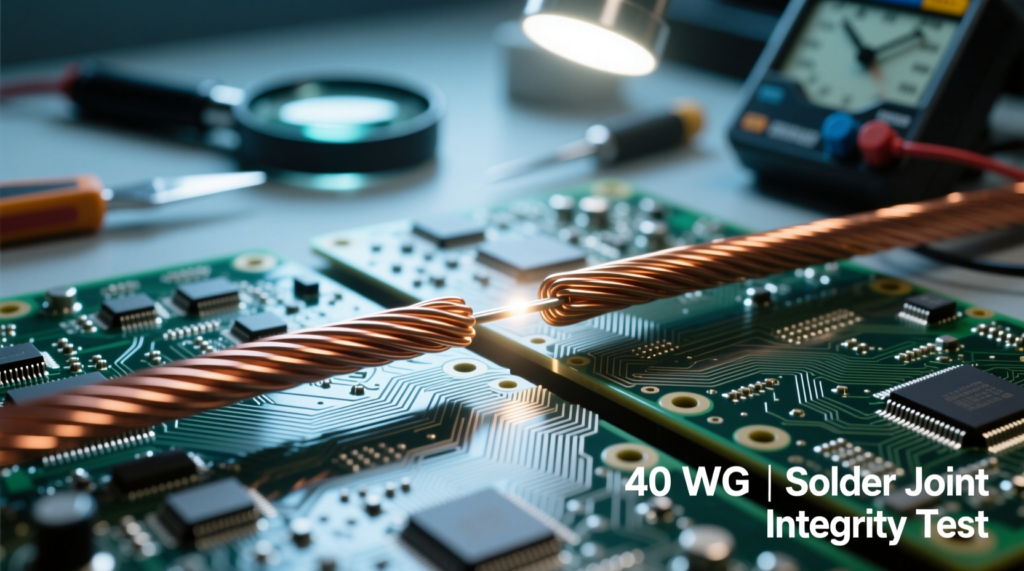


When it comes to how to jumper broken PCB trace with 40 AWG enamel copper wire, getting the right details matters. Recommended Products:
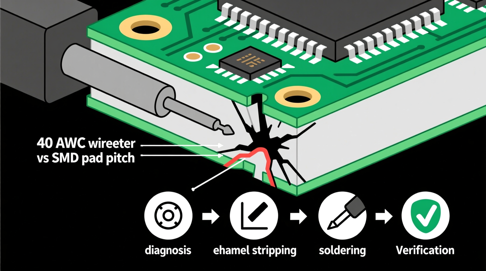
Andonstar AD246S‑M Digital HDMI Microscope
FNIRSI LCR‑ST1 Smart LCR Tweezers
40 AWG Solderable Enamel Copper Wire
A broken PCB trace is not a missing component. It is an open net hiding under solder mask, between two pads, vias, or component leads, on a board packed with SMD parts that laugh at your standard multimeter probes. The fix is not a blob of solder and a prayer. It is a controlled bridge made from 40 AWG enamel copper wire, laid down under magnification, verified with the right diagnostic tools, and anchored so it survives the next thermal cycle.
This guide shows you how to diagnose the open, strip and tin the wire, place the jumper, and verify the repair without converting a recoverable fault into a scrapped motherboard.
1. The Technical Reality: What Actually Fails on a Modern PCB
The Failure Mode
A modern multi-layer PCB fails as an single open circuit on one net. Copper trace severance or partial delamination breaks the path between two conductive points. The board looks fine. The components test fine. One net simply does not conduct.
Root-Cause Sequences to Map Before Touching the Board
Mechanical flexure stress cracks the trace or via barrel.
Overcurrent thermal burnout vaporizes a section of the copper path.
Corrosion at via barrels or pad edges eats through the conductor.
Pad lifting during component removal tears the trace away from its anchor.
Latent manufacturing defects in high-density motherboards leave weak points that fail months or years later.
Why the Failure Hides
Adjacent SMD components must be ruled out first. A resistor, capacitor, or IC pin can look like a trace fault when it is actually the failed part. The break is usually confirmed with smart LCR tweezers or a bench multimeter in continuity mode after the surrounding components check out.
Why 40 AWG Is the Consensus Upper Limit for Fine-Pitch Work
Technicians on repair forums report the same problem repeatedly: 30 AWG or 28 AWG jumper wire bridges across neighboring pads on dense laptop motherboards and game-console boards. The diameter is simply too large for modern SMD pitch.
40 AWG enamel copper wire solves this. The nominal bare conductor diameter is approximately 0.079 mm (0.0031 in), and the total coated diameter sits between 0.084 mm and 0.089 mm depending on whether the enamel is single or heavy build.
That thin profile fits inside tight pitch constraints, while the enamel insulation prevents accidental contact with nearby traces.
Operational Risks That Convert a Simple Open into an Unrecoverable Board
Incomplete enamel removal leaves a resistive film, producing cold joints or intermittent continuity.
Excessive heat or mechanical tension lifts adjacent traces, delaminates pads, or damages solder mask on multi-layer boards.
The margin for error is small. The right gear and technique make the difference between a working board and a donor board.
2. The Core Gear Architecture: Validated Repair Stack
2.1 High-Clearance Digital Microscope
Andonstar AD246S‑M Digital HDMI Microscope
| Feature | Specification |
|---|---|
| Display | 7-inch LCD |
| Video Output | 2160P |
| Bracket Height | 30 cm vertical clearance |
| Lenses | Three interchangeable options |
| Output | Dual-screen HDMI |
| Lighting | LED ring illumination |
Cheap digital microscopes with short vertical brackets force the soldering iron to collide with the lens housing. That collision makes trace-level work impossible. The 30 cm bracket on the AD246S‑M gives you room to work underneath the optics with a fine iron, hot-air nozzle, or tweezers.
2.2 Smart LCR Tweezers for In-Circuit Diagnosis
FNIRSI LCR‑ST1 Smart LCR Tweezers
| Feature | Specification |
|---|---|
| Display | 1.14-inch color screen |
| Weight | 41 g |
| Test Frequencies | 100 Hz / 1 kHz / 10 kHz |
| Test Voltages | 0.3 V (In-circuit) / 0.6 V (High clarity) |
| Battery | 250 mAh Li-ion with USB charging |
| Tips | Gold-plated micro-tips |
Handheld probes are too large and too blunt for in-circuit SMD testing.
They touch multiple pads at once, and parallel semiconductor junctions conduct under test voltage, giving false readings. The LCR‑ST1’s micro-tips and low-voltage 0.3 V mode isolate the part or trace you actually want to measure.
2.3 40 AWG Solderable Enamel Copper Wire
40 AWG Solderable Enamel Copper Wire
| Parameter | Value |
|---|---|
| Bare Conductor Diameter | ~0.079 mm (0.0031 in) |
| Coated Diameter | ~0.084 mm–0.089 mm |
| Resistance | ~3.44 Ω/m |
| Current Capacity | Low milliampere range |
| Application | Signal traces; not high-current rails |
| Insulation | Enamel (thermal/mechanical strip required) |
2.4 Fine-Pitch Soldering Station
Use a temperature-controlled station set to 300 °C–350 °C.
That range is hot enough for reliable enamel burn-off and lead-free solder wetting, but controlled enough to avoid cooking the board.
Tip geometry matters. Choose 0.2 mm–0.4 mm conical or bevel tips for trace-level work. A blunt chisel tip will bulldoze pads and adjacent components.
2.5 Auxiliary Consumables
No-clean flux pen or liquid rosin flux.
Solder wick for pad cleanup.
Fine-tip anti-static tweezers.
Silicone or heat-resistant work mat.
UV-curing solder mask or high-temperature adhesive for securing the jumper.
3. The Technical Setup Blueprint: From Diagnosis to Jumper
3.1 Pre-Repair Diagnostics and Net Isolation
Start with a visual inspection under magnification. Look for lifted pads, burned solder mask, or cracked traces. Then rule out adjacent shorted or open SMD components. Only after the surrounding parts check out should you isolate the affected net and confirm the open with LCR tweezers or a bench multimeter in continuity mode.
3.2 Enamel Stripping and Pre-Tinning
Strip the enamel at the intended solder points using one of these methods: Thermal burn-off at 300 °C–350 °C with a fine soldering iron, or mechanical scraping with a scalpel or craft knife under magnification.
Verify that solder fully wets the copper after stripping. If the enamel is still present, the solder will bead up instead of flowing.
Forum-approved shortcut: Pre-tin the 40 AWG wire and scrape the enamel at the intended solder points before placement. This reduces rework, keeps the iron off the board longer, and lowers the chance of trace damage.
3.3 Jumper Placement and Soldering
Check out TECH Collection Amazon Products
Cut the 40 AWG wire to the shortest practical length. Shorter wire means lower inductance and less chance of snagging.
Position the wire under a high-magnification stereomicroscope with adequate vertical working clearance. Solder one end, then the other, using minimal dwell time and no-clean flux to improve wetting.
Avoid excessive heat or mechanical tension. Either one can lift adjacent traces or delaminate internal plane connections on multi-layer boards.
3.4 Routing and Mechanical Securing
Route the jumper along the solder mask, keeping it clear of neighboring traces and pads. Secure the wire to the solder mask with small dabs of UV-curing solder mask or high-temperature adhesive after soldering.
This mechanical anchor prevents future flexure fatigue and protects against accidental shorts.
3.5 Verification Workflow
Re-test continuity across the repaired net.
Verify no shorts to adjacent nets.
Confirm stable readings under gentle mechanical prodding.
If the reading flickers when you tap the wire, you have a cold joint or an unanchored bridge. Reflow and secure it.
4. Field Verdict & Operational ROI
The Cost of Getting It Wrong
A single overheated multi-layer board can turn a simple open trace into an unrecoverable failure. That means scrapping an expensive motherboard, game console, or industrial controller. The repair forums are full of boards killed by blunt tips, thick wire, cheap microscopes, and too much heat.
Why the Validated Stack Pays for Itself
The right microscope clearance, precision tweezers, and temperature-controlled iron eliminate the false starts, lifted traces, and intermittent joints that dominate repair-forum horror stories. You buy the gear once. You save the board once. After that, the stack has paid for itself.
Bottom Line
For high-density PCB trace repair, the combination of the Andonstar AD246S‑M Digital HDMI Microscope, FNIRSI LCR‑ST1 Smart LCR Tweezers, certified 40 AWG Solderable Enamel Copper Wire, and a 0.2 mm–0.4 mm fine-pitch soldering station is the minimum professional-grade architecture that reliably converts an open net back into a working circuit.
Conclusion
Community Reference & Authority Resources:
You now have a complete blueprint for jumpering a broken PCB trace with 40 AWG enamel copper wire. You know how the failure forms, why 40 AWG is the practical upper limit for dense boards, which tools give you accurate diagnosis and safe soldering, and how to verify the repair before it leaves your bench.
The real value is not just fixing one trace. It is building a repeatable repair capability that rescues boards that would otherwise be written off. With the right stack, a steady hand, and the process above, an open net becomes a solved problem.
🔍 Explore More: See all tech guides and tutorials for how to jumper broken PCB trace with 40 AWG enamel copper wire.
Check out TECH Collection Amazon Products