





When it comes to troubleshooting motherboard trace damage after liquid spill repair guide, getting the right details matters. Recommended Products:
Andonstar AD246S-M Digital HDMI Microscope
FNIRSI LCR-ST1 Smart LCR Tweezers
iSonic P4820-WSB Ultrasonic Cleaner
Troubleshooting Motherboard Trace Damage After Liquid Spill: The 2026 Repair Guide for Corrosion, Dendrites, and Hidden Failures
A laptop that boots after a spill is not a repaired laptop. It is a laptop that has not finished failing. The liquid you cannot see—trapped under solder mask, inside vias, under BGA packages, and beneath RF shields—keeps working long after the visible droplets are gone. Ionized contaminants set up tiny electrolytic cells across the board. Copper dissolves. Dendrites grow. Inner-layer traces corrode from the inside out. If you stop at “it dried and turned on,” you are leaving the real damage untreated. This guide shows you how to diagnose, clean, repair, and verify a liquid-damaged motherboard with the same workflow used by professional bench technicians in 2026.
The Technical Reality / The Failure Point
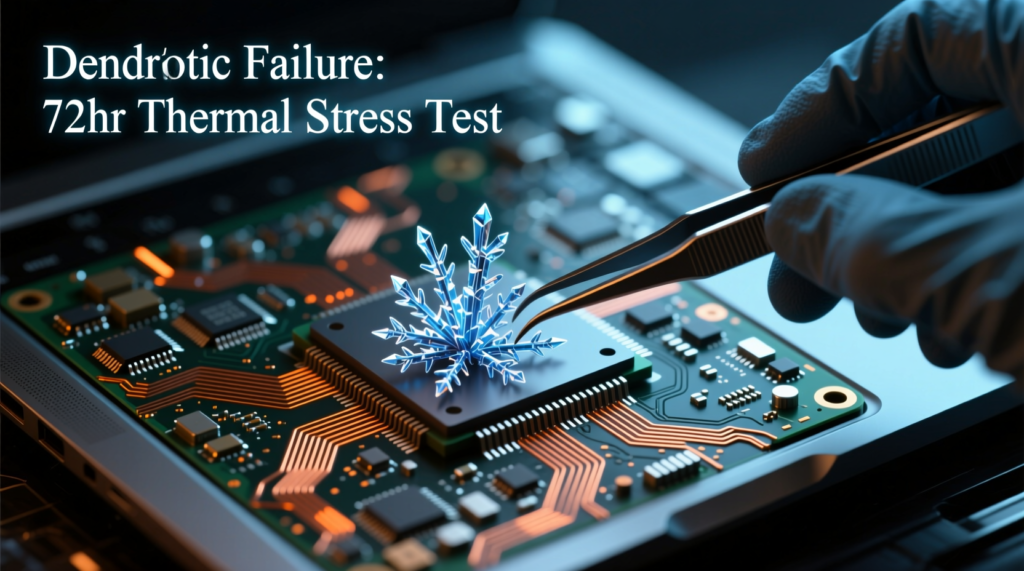
Electrochemical Corrosion Is the Real Killer—Not Just a “Wet Circuit”
Ionized contaminants from water, coffee, soda, and saltwater create electrolytic cells between copper traces, vias, pads, and component leads.
That means the spill is not merely conducting electricity where it should not. It is actively dissolving metal. Water plus salts, sugars, or minerals becomes an electrolyte. When it bridges two conductors at different potentials, current flows and metal migrates from anodic sites into the solution.
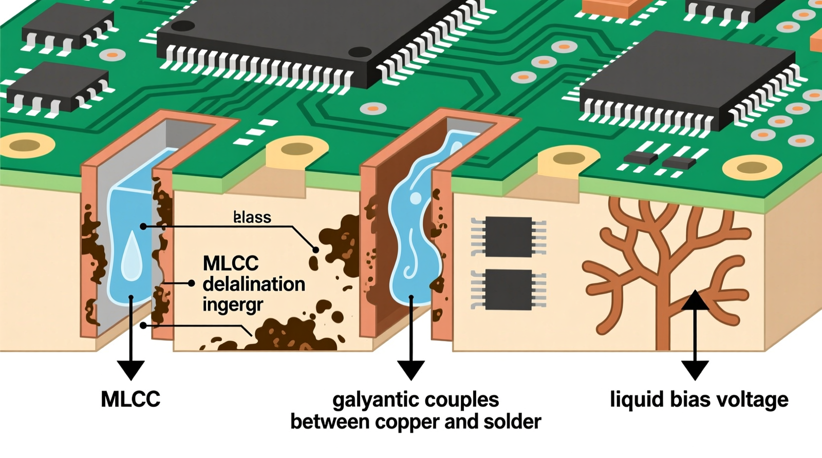
Dissimilar-metal galvanic couples—copper trace + tin/lead solder + nickel underplating—accelerate metal dissolution.
In practical terms, every plated through-hole, every pad, and every trace edge becomes a battery terminal. The copper loses mass. Solder joints turn powdery. Nickel underplating corrodes. The result is open traces, high-resistance joints, and latent failures that surface days or weeks later.
Dendritic Growth and Conductive Filament Formation
Residual ionic film under solder mask or between closely spaced SMD pads enables metal migration under bias voltage.
Even a clean-looking board can carry an invisible film of ionic residue. Once voltage is applied, dissolved metal ions migrate toward the cathode and plate out as tiny filaments.
Dendrites bridge power and ground rails, data lines, and feedback networks.
The impact is intermittent shorts, thermal runaway, and secondary component failure. A board can pass a short test at room temperature and then crash under load when a dendrite grows hot enough to conduct.
Trace, Via, and SMD Degradation Pathways
Copper traces narrow or neck at stress points; vias corrode from the inside out, creating hidden open circuits.
A via is a vertical barrel of copper connecting layers. Liquid wicks down the barrel. The corrosion starts inside the hole where you cannot see it and where a multimeter probe cannot reach.
Multi-layer boards conceal damaged inner-layer traces—surface continuity checks are unreliable without component-level probing.
You can measure continuity between two surface pads and read “good” while an inner layer is eaten through. Surface measurements lie. You need visual inspection plus component-level probing.
MLCCs absorb moisture and crack, becoming shorted or leaky.
Multi-layer ceramic capacitors are micro-laminates. Moisture ingress causes internal delamination or cracking. A cracked MLCC can short rail to ground and take out a voltage regulator.
MOSFETs and PMICs fail when corrosion penetrates package leads, causing low-side/high-side shorts and blown power rails.
Power MOSFETs and PMICs sit on the highest-current paths. Corroded leads raise resistance, generate heat, and eventually short. One shorted high-side MOSFET can dump battery voltage into a 1.05 V rail and destroy every downstream IC.
Connectors and FPC sockets corrode, raising contact resistance or breaking signal paths entirely.
Liquid pools in connectors. Pins tarnish. Flex cable contacts oxidize. The result is charging issues, display failures, and intermittent peripherals that look like software bugs.
Secondary Thermal Damage and Solder-Mask Delamination
Powering on a contaminated board drives high current through unintended paths, burning traces and lifting solder mask.
This is why the “rice bag” or “leave it in the sun” approach is dangerous. If the board powers on while conductive residue remains, you can burn a trace in seconds. The damage becomes worse than the original spill.
Moisture absorption weakens the epoxy-glass interface; hot-air rework or mechanical cleaning lifts pads and exposes inner-layer copper.
Once the board is waterlogged, even normal rework heat can pop pads. That is why controlled thermal profiles matter more after liquid damage than on a fresh board.
The Core Gear Architecture (2026 Validated Stack)
Visual Inspection Layer: Andonstar AD246S-M Digital HDMI Microscope
7-inch built-in LCD + 2160P HDMI video output.
You need to see dendrites, lifted pads, and cracked MLCCs at high magnification without losing context. The 2160P output gives you the resolution to spot a hairline crack in a 0402 capacitor.
30 cm high working bracket for hot-air nozzle and iron clearance.
This is the spec that matters for rework. Cheap USB microscopes sit so low that you cannot fit a hot-air nozzle or soldering iron under the lens. The 30 cm bracket lets you solder while you watch.
Three interchangeable lenses (A / D / L) for different working distances and magnifications.
Different jobs need different fields of view. A wide scan for corrosion, a mid lens for trace routing, and a long-distance lens for hot-air work.
Dual-screen HDMI architecture: local LCD stays active while outputting to an external monitor.
You can let a colleague or camera watch the external screen while you keep the live view in front of you.
LED ring illumination, continuous magnification, metal stand with fine-focus rack.
Consistent lighting and stable focus are non-negotiable when you are bridging a 40 AWG wire across a 0.2 mm trace.
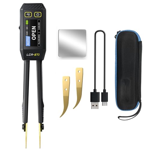
Component Characterization Layer: FNIRSI LCR-ST1 Smart LCR Tweezers
1.14-inch color display, 41 g mass, built-in 250 mAh lithium battery.
It is light enough to use one-handed while you hold the board with the other. That matters when you are probing under a microscope.
Check out TECH Collection Amazon Products
Selectable test frequencies: 100 Hz / 1 kHz / 10 kHz.
Different frequencies reveal different component behaviors. A capacitor may look fine at 100 Hz and fail at 10 kHz.
Dual test voltages: 0.3 V and 0.6 V for in-circuit measurement without forward-biasing adjacent semiconductor junctions.
This is the critical feature. A standard multimeter shoves 2–3 V across a component. On a populated board, that turns on surrounding diodes and transistors and gives you a fake reading. The 0.3 V mode stays below the silicon turn-on threshold, so you measure the actual resistor or capacitor.
Gold-plated micro-tips; resistance, capacitance, inductance, and diode health modes.
The fine tips let you isolate a single 0402 or 0201 part. Standard probes short across three components at once.
Rework Thermal Layer
Hot-air rework station (Quick 861DW or ATTEN ST-862D class):
| Feature | Specification |
|---|---|
| Heater | 1000 W |
| Temperature Range | 100 °C–500 °C |
| Airflow | 20–120 L/min |
| Display | Digital |
| Nozzles | Quick-change (3 mm–10 mm) |
A 1000 W closed-loop heater recovers fast when you open the oven door, so to speak. The 3 mm nozzle focuses heat on a single QFN; the 10 mm nozzle handles large shield cans or connectors. Airflow from 20–120 L/min lets you desolder tiny SMDs without blowing them off the board.
Precision soldering iron—Hakko FX-888D:
| Feature | Specification |
|---|---|
| Heater | 70 W ceramic |
| Temperature Range | 120 °C–899 °F / 50 °C–480 °C |
| Safety | ESD-safe, digital control |
70 W gives fast recovery when you touch a large ground plane. Digital control keeps the tip at the exact temperature you set, which protects already-weakened pads.
Cleaning and Decontamination Layer
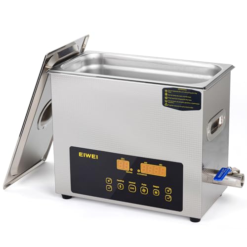
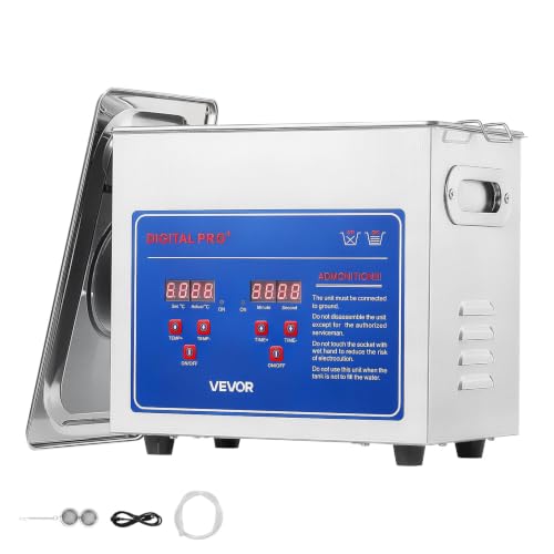
Ultrasonic cleaner—iSonic P4820-WSB:
| Feature | Specification |
|---|---|
| Tank | 2.5 L stainless |
| Frequency | 42 kHz transducer |
| Heater | Integrated to ~65 °C |
42 kHz is the sweet spot for PCB cleaning. It is aggressive enough to dislodge ionic residue under shields and inside connectors, but gentle enough not to damage delicate components. The 2.5 L tank fits most laptop motherboards flat.
Chemistry: 99 % isopropyl alcohol, deionized water, no-clean or water-soluble flux.
Do not use tap water. Minerals and chlorine leave conductive residue. Do not use vinegar or cola. The community consensus is 99 % isopropyl alcohol and deionized water, with ultrasonic agitation.
Trace Repair Consumables
40 AWG / 0.02 mm enameled copper jumper wire, polyurethane insulation, 155 °C rating.
This is thinner than a human hair. It lets you bridge damaged traces without adding mass or shorting adjacent pads. The polyurethane enamel burns off cleanly when tinned.
Sn63/Pb37 or SAC305 solder wire, 0.3 mm–0.5 mm diameter.
Recommended Insights From Our Guide Library:
- The Art of Revival: Repairing Liquid-Damaged Electronics at the Component Level » Z A D A
- The Ultimate Guide to Motherboard Trace Repair: Creative Fixes for Open Circuits » Z A D A
- Circuits » Z A D A
- The Art and Science of Repairing Broken Traces on Printed Circuit Boards (PCBs) » Z A D A
- electronics repair
Fine solder gives you control. Sn63/Pb37 flows at lower temperatures and is forgiving on damaged pads. SAC305 is lead-free and required for RoHS-compliant repairs, but needs higher heat.
Acrylic-based conformal coating—e.g., MG Chemicals 422B—for repaired areas.
After repair, you re-seal the board. MG Chemicals 422B puts a moisture-resistant barrier over exposed copper and jumper wires, blocking future dendritic growth.
ESD and Power Safety
Grounded ESD mat and wrist strap with 1 MΩ current-limiting resistor.
Liquid damage already weakened components. A static discharge through a MOSFET gate can finish the job. The 1 MΩ resistor limits current to ground if you touch live mains.
Bench DC power supply with adjustable current limiting for post-repair power-up.
Never power a repaired spill board from its own battery first. A bench supply lets you set a current limit so a hidden short only trips the supply, not the entire rail.
The Technical Setup Blueprint
Step 1 — Pre-Power Visual Inspection
Inspect under microscope for corrosion, burned traces, and lifted pads.
Look for white or green powder around connectors, green crust on vias, and blackened copper where a trace burned. The Andonstar AD246S-M Digital HDMI Microscope at high magnification reveals what the naked eye misses.
Remove shields, connectors, and BGA-adjacent metalwork—liquid pools where visual inspection cannot reach.
RF shields, heatsink brackets, and connector housings hide pooled liquid. You must remove them. If you skip this, you are cleaning only the surface.
Step 2 — Ultrasonic Cleaning and Drying
Run 42 kHz bath at ~65 °C for 5–15 minutes depending on contamination severity.
A light water spill may need 5 minutes. Coffee, soda, or saltwater can need 15 minutes or multiple cycles. The iSonic P4820-WSB Ultrasonic Cleaner at 42 kHz and 65 °C loosens residue without damaging the board.
Final rinse: deionized water, then 99 % isopropyl alcohol.
Deionized water removes the cleaning solution. Isopropyl alcohol displaces the water and evaporates cleanly.
Dry at 60 °C–80 °C for 30–60 minutes before applying power.
Moisture under BGA packages and inside connectors will not evaporate at room temperature. A controlled bake drives it out.
Step 3 — In-Circuit SMD Testing with LCR Tweezers
Use FNIRSI LCR-ST1 Smart LCR Tweezers in 0.3 V mode to avoid turning on surrounding silicon.
This is where most DIY repairs go wrong. A multimeter in diode mode will tell you a capacitor is shorted because it sees the surrounding diodes. The 0.3 V mode isolates the component.
Isolate 0402/0201 components—standard multimeter probes cannot resolve single parts on populated boards.
The LCR tweezers’ fine tips grab one component at a time. You can measure a suspect MLCC while the rest of the circuit stays connected.
Step 4 — Continuity and Short-Circuit Mapping
Combine multimeter probing with microscope-guided inspection.
Buzz out power rails to ground. If you find a short, use the microscope to look for dendrites, solder bridges, or cracked MLCCs on that rail.
Map hidden inner-layer trace failures and via corrosion.
If two surface pads read open but the schematic says they should connect, suspect a via. You may need to drill or scrape the via carefully and bridge it with 40 AWG wire.
Step 5 — Trace Repair and Rework Execution
Route 40 AWG jumper wire across damaged traces.
Strip the enamel by tinning the ends, then solder the jumper from a good pad to a good pad. Keep the wire as short and low as possible.
Match hot-air nozzle (3 mm–10 mm) and set airflow/temperature for component size.
A 3 mm nozzle at 350 °C with moderate airflow removes a tiny SMD. A 10 mm nozzle at 400 °C with higher airflow removes a large connector. Match the tool to the job or you lift pads.
Iron temperature: 350 °C–380 °C for Sn63/Pb37; 380 °C–420 °C for SAC305 lead-free.
Lead-free solder needs more heat, but damaged boards tolerate less. Preheat the board if possible.
Optional preheat plate for large ground-plane boards to reduce thermal shock.
A preheat plate brings the whole board to 100 °C–150 °C. That reduces the delta-T when you apply hot air, so pads and traces are less likely to lift.
Step 6 — Conformal Coating and Final Protection
Check out TECH Collection Amazon Products
Apply MG Chemicals 422B acrylic conformal coating over repaired traces.
Brush or spray a thin layer over exposed copper and jumper wires. This seals out moisture and ionic contamination.
Protect against residual ionic films and future dendritic growth.
Even after cleaning, microscopic residue can remain. The conformal coating adds a dielectric barrier that stops dendrites from forming.
Step 7 — Current-Limited Power-Up and Functional Verification
Use bench DC supply with adjustable current limiting for first power-on.
Set the voltage to the battery rail or main rail and the current limit low. If the board draws more than expected, the supply folds back. You find the short before anything burns.
Verify rails, boot behavior, and thermal stability before returning to service.
Check each regulator output with a scope or multimeter. Boot the OS. Run a stress test and watch for hot spots with a thermal camera or your fingertip.
Field Verdict & Operational ROI
Why “It Worked After Drying” Is a Trap
Boards that boot post-spill often fail later as corrosion continues under solder mask and inside connectors.
The visible liquid is gone, but the electrolyte remains. Every hour the board runs, the corrosion continues. The failure may not appear for weeks.
Full disassembly, ultrasonic cleaning, and drying are non-negotiable.
If a customer tells you “it dried and worked,” that is the beginning of the repair, not the end.
The Cost of Cheap Microscopes and Uncontrolled Heat Guns
Low-cost USB microscopes have short working distances and high latency—impossible for simultaneous soldering and viewing.
You cannot position a hot-air nozzle under a microscope that sits 5 cm from the board. You cannot solder what you cannot see in real time.
Uncontrolled heat guns lift weakened pads and delaminate traces; closed-loop stations are mandatory for laptop motherboard work.
A hardware-store heat gun has no temperature feedback. It will overheat one spot while the rest of the board stays cold, popping pads that the liquid already weakened.
ROI of the 2026 Gear Stack vs. Secondary Damage
The Andonstar AD246S-M Digital HDMI Microscope + FNIRSI LCR-ST1 Smart LCR Tweezers + Quick/ATTEN hot-air + Hakko FX-888D stack prevents VRM, PMIC, and controller IC destruction.
Spending a few hundred dollars on the right tools prevents thousands of dollars in destroyed motherboards. One saved laptop motherboard pays for the microscope.
Correct chemistry and ultrasonic cleaning eliminate latent corrosion that causes repeat failures.
A board that comes back two weeks later with the same fault costs you reputation and labor. Do it right once.
When to Invest in the Full Stack vs. When Replacement Wins
Multi-layer boards with inner-layer damage or delaminated pads may exceed practical repair thresholds.
If multiple inner layers are blown, if pads are missing across a wide area, or if the board is warped, the repair may take longer than a replacement board costs.
Use the full diagnostic workflow to make a data-driven repair-or-replace decision.
The workflow itself tells you when to stop. If you cannot establish reliable power rails after cleaning and trace repair, you have the evidence to recommend replacement.
Conclusion
Community Reference & Authority Resources:
Liquid-spill motherboard repair is an electrochemical problem, not a drying problem. Ionized residue drives corrosion under solder mask, inside vias, and between SMD pads. Dendrites grow. Traces open. Components short. The only reliable path is a complete workflow: visual inspection with a tall-bracket microscope, ultrasonic cleaning with the right chemistry, in-circuit component testing with low-voltage LCR tweezers, controlled thermal rework, trace repair with 40 AWG jumper wire, conformal coating protection, and current-limited power-up verification.
The 2026 gear stack—Andonstar AD246S-M Digital HDMI Microscope, FNIRSI LCR-ST1 Smart LCR Tweezers, iSonic P4820-WSB Ultrasonic Cleaner, Quick/ATTEN hot-air station, and Hakko FX-888D—is not a collection of accessories. It is an operational investment that prevents secondary thermal damage and repeat failures. Use it to turn “it worked after drying” into a fully verified, long-lasting repair.
🔍 Explore More: See all tech guides and tutorials for troubleshooting motherboard trace damage after liquid spill repair guide.
Check out TECH Collection Amazon Products